Home
» New Trends
»
Next-Gen Semiconductors for AI and Supercomputing: What Matters Beyond FLOPS
Next-Gen Semiconductors for AI and Supercomputing: What Matters Beyond FLOPS
In 2026, the most important change in AI and supercomputing hardware is not a single new transistor node or accelerator. It is the shift toward designing the entire compute system as one semiconductor platform: logic, high-bandwidth memory, chiplets, package, scale-up links, network fabric, power delivery, cooling, and software all have to be co-optimized. NVIDIA says its Vera Rubin platform is now in full production, AMD launched its Instinct MI400 family in July 2026, Micron is shipping HBM4 in volume, and TSMC says N2 entered high-volume manufacturing in late 2025 while N2P and A16 are scheduled for volume production in the second half of 2026. Those developments make one lesson clear: choosing next-generation semiconductors now means choosing a system architecture, not just a chip.
That matters because the “best” semiconductor depends heavily on the workload. A frontier-model training cluster, a national supercomputing center, a cloud inference service, and an enterprise AI deployment can all favor different trade-offs. Peak FLOPS alone is a poor purchasing rule. Memory capacity, memory bandwidth, interconnect topology, supported numerical formats, software maturity, cooling requirements, availability, and total system cost can matter just as much.
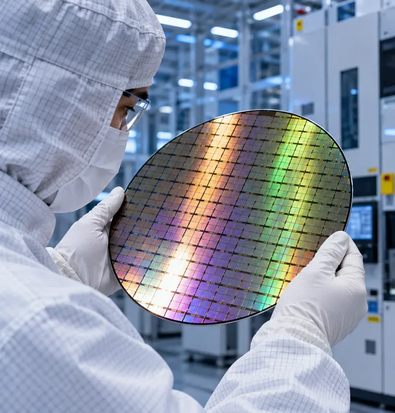
A cleanroom technician inspects a patterned silicon wafer, illustrating the precision manufacturing behind advanced processors used in AI and high-performance computing.
The 2026 shift: memory and interconnect are now first-class design constraints
Modern AI accelerators can perform arithmetic faster than data can always be supplied to them. That makes memory bandwidth and data movement central to real-world performance. Micron states that its HBM4 36GB 12-high product is in high-volume production and delivers more than 2.8 TB/s of bandwidth per stack, using a 2,048-bit interface, with more than 20% better power efficiency than its comparable HBM3E product. See Micron's HBM4 product information and its March 2026 HBM4 production announcement.
The trade-off is that HBM is expensive and packaging-intensive. More stacks increase capacity and bandwidth, but they also enlarge the package, complicate routing and power delivery, increase thermal density, and place more pressure on packaging yield. For memory-bound inference, large recommendation models, long-context LLM serving, and scientific workloads with high data reuse, paying for more HBM can make sense. For smaller models with low memory pressure, that premium may be wasted.
Option 1: integrated GPU rack systems for maximum AI scale
NVIDIA's Vera Rubin NVL72 illustrates the system-first approach. NVIDIA publishes a configuration of 72 Rubin GPUs and 36 Vera CPUs, with 20.7 TB of HBM4 across the rack. A single Rubin GPU is listed with 288 GB of HBM4, while NVLink 6 provides up to 3.6 TB/s of scale-up bandwidth per GPU. The platform is designed for pretraining, post-training, test-time scaling, and large-scale agentic inference. Current specifications are available on the NVIDIA Vera Rubin NVL72 page.
The advantage is integration. Compute, CPU-GPU coherence, scale-up fabric, networking, system management, and software are engineered together. That can reduce the risk of assembling a large cluster from independently optimized components. It is particularly attractive when time-to-deployment and a mature GPU software ecosystem matter more than architectural openness.
The trade-off is commitment to a tightly integrated platform. Large rack-scale systems also demand significant facility planning, including liquid cooling, electrical distribution, and network design. Buyers should compare delivered application throughput per rack and per megawatt, not only accelerator specifications. Vendor-published peak performance numbers are theoretical or workload-specific and should be validated with the actual model, batch size, sequence length, numerical precision, and communication pattern that will run in production.
Option 2: chiplet-heavy GPU systems with a more open infrastructure strategy
AMD's Instinct MI400 series takes a different route while pursuing the same system-level goal. The MI455X combines chiplets, HBM4, advanced packaging, and Infinity Fabric. AMD lists up to 432 GB of HBM4 and up to 23.3 TB/s of peak theoretical memory bandwidth per MI455X GPU. The Helios rack-scale reference design combines 72 MI455X GPUs and is built around open infrastructure standards. AMD says volume deployments based on Helios are expected in the second half of 2026. See the AMD Instinct MI400 series page.
This approach is appealing when memory capacity, chiplet modularity, ROCm, and open rack or interconnect standards are strategic priorities. More local HBM can reduce model partitioning pressure and may help inference workloads with large KV caches or workloads that would otherwise spill data across accelerators.
The trade-off is software validation. A platform can have strong silicon specifications but still require engineering work if a critical framework, kernel, collective communication pattern, or custom operator is better optimized elsewhere. Organizations considering AMD should benchmark their own training and inference pipelines under ROCm rather than assuming portability automatically means equal performance.
Option 3: specialized AI ASICs when workload fit matters more than generality
Google's TPU7x, also known as Ironwood, shows the benefits of a domain-specific accelerator. Google Cloud lists 192 GB of HBM per chip, about 7.38 TB/s of HBM bandwidth, 1.2 TB/s of bidirectional inter-chip interconnect bandwidth, and large pod configurations. The architecture is built around tensor and sparse compute rather than trying to serve every possible accelerator use case. Technical details are available in the Google Cloud TPU7x documentation.
A specialized accelerator can be a strong choice when the target models map cleanly to its compiler, numerical formats, memory hierarchy, and supported frameworks. Cloud delivery can also remove much of the facility burden associated with owning a large AI cluster.
The trade-off is portability and workload breadth. If an organization relies on low-level CUDA-specific code, unusual kernels, niche scientific libraries, or applications outside the accelerator's sweet spot, migration cost can outweigh hardware efficiency. The correct comparison is therefore end-to-end time-to-result and cost-to-result for the actual software stack.
Advanced packaging is becoming as important as transistor scaling
The leading AI processors are too complex to treat packaging as a passive final step. TSMC's CoWoS platform integrates logic and HBM using large interposers, while its SoIC technology supports 3D chip stacking with high-density die-to-die connections. TSMC states that its 3nm SoIC stacking entered volume production in 2025. Its CoWoS-L technology has also scaled beyond conventional reticle-size limitations for large AI and HPC packages. See TSMC's official CoWoS and SoIC technology pages.
Intel Foundry is pursuing a similar objective with EMIB and Foveros. EMIB uses embedded silicon bridges to connect dies at high density without requiring a full silicon interposer across the entire package. Foveros adds vertical stacking, while Foveros Direct uses copper-to-copper hybrid bonding for very fine die-to-die connections. Intel describes these technologies on its advanced packaging page.
The engineering choice is not simply “2.5D versus 3D.” Designers have to balance interconnect density, package size, thermal behavior, known-good-die strategy, yield, assembly complexity, and cost. A 3D stack can shorten links and improve bandwidth density, but vertically stacking hot compute dies can make heat removal harder. A 2.5D architecture can be easier to cool and test but may require a larger footprint and longer interconnects.
Leading-edge process nodes still matter—but for specific reasons
Transistor scaling remains important because AI and HPC systems are power-limited. TSMC says its N2 technology entered volume production in the fourth quarter of 2025, using nanosheet transistors, and that N2P and A16 are scheduled for volume production in the second half of 2026. A16 adds backside power delivery, which moves power routing away from the front-side signal layers and is aimed at demanding HPC designs with dense power networks. See the TSMC A16 technology page.
Intel's 18A node similarly combines a gate-all-around transistor architecture, branded RibbonFET, with backside power delivery, branded PowerVia. Intel said in June 2026 that 18A had entered production in 2025 and that 18A-P had entered risk production. See Intel Foundry's 2026 process update.
The trade-off is maturity versus maximum efficiency. A new node can improve performance, density, or power, but mature nodes often offer better yield, lower cost, and a more established design ecosystem. Chiplet architectures make this choice less binary: compute tiles can use the newest node while I/O, cache, analog, or interface dies remain on older, cheaper processes.
Open chiplet standards can reduce lock-in, but interoperability is not automatic
UCIe is designed to standardize high-speed die-to-die communication between chiplets. UCIe 3.0 supports 48 GT/s and 64 GT/s data rates, doubling the maximum data rate of UCIe 2.0, while maintaining backward compatibility. It also extends manageability and power-saving features. The specification overview is available from the UCIe Consortium.
For semiconductor designers, UCIe can make it easier to combine chiplets from different teams, processes, or eventually suppliers. For system buyers, however, an open die-to-die standard does not immediately translate into interchangeable accelerator modules. Packaging, power, firmware, memory interfaces, thermal design, security, validation, and software still have to align. UCIe should therefore be viewed as an important building block for modular design rather than a guarantee of plug-and-play silicon.
What should you choose for different AI and supercomputing needs?
Chiplet flexibility, foundry access, packaging ecosystem, open interconnects
Heterogeneous chiplets with advanced 2.5D/3D packaging
NRE cost, validation time, packaging capacity and yield
How to evaluate a next-gen semiconductor platform without being misled by headline specs
Start with the workload, not the chip. Measure model size, active parameter count, context length, batch size, communication intensity, precision requirements, checkpointing behavior, and expected utilization. Then evaluate the hardware against those constraints.
For compute-bound workloads: compare sustained kernel performance at the precision you will actually use, not only peak FP4 or FP8 figures.
For memory-bound workloads: prioritize effective HBM bandwidth, capacity, cache behavior, and data movement overhead.
For distributed training: measure collective operations such as all-reduce and all-to-all at the intended node count.
For inference: test tokens per second, time to first token, inter-token latency, concurrency, and energy per request using realistic context lengths.
For HPC: verify FP64, vector performance, memory behavior, compiler quality, MPI scaling, and the exact scientific libraries in use.
For facilities planning: include rack power, cooling technology, floor loading, network optics, serviceability, and spare capacity.
This is especially important in 2026 because vendor architectures are diverging. NVIDIA's Rubin platform emphasizes tightly integrated rack-scale compute and networking; AMD's MI400 family combines large HBM4 capacity with chiplets and an open-infrastructure strategy; Google TPU7x targets tensor-centric workloads through a cloud-delivered ASIC; TSMC, Intel, memory vendors, and standards bodies are simultaneously changing the physical building blocks underneath all of them.
The practical conclusion: optimize the whole data path
The next generation of semiconductors will power AI and supercomputing not because one device wins every benchmark, but because the industry is learning to move data more efficiently from storage to CPU, from CPU to accelerator, between accelerators, and between stacked dies and HBM. HBM4, chiplets, 2.5D and 3D packaging, backside power delivery, fast scale-up links, and open die-to-die standards are all responses to the same constraint: arithmetic is only useful when data arrives fast enough and within the available power budget.
For organizations buying infrastructure today, the safest recommendation is workload-specific. Choose an integrated GPU platform when ecosystem maturity and rapid scale are the priority. Consider an open GPU platform when memory capacity, infrastructure flexibility, and software portability are strategic. Use a specialized ASIC when the workload maps cleanly to it and cloud or platform dependency is acceptable. For custom silicon, invest in chiplets and advanced packaging when the performance and product-volume gains justify the extra design and validation complexity.
Most importantly, benchmark complete systems under production conditions. The semiconductor that looks fastest on a specification sheet may not be the one that delivers the lowest cost, shortest time-to-result, or best performance per watt for your workload.