Home
» New Trends
»
Inside the Global Race for Advanced Chip Packaging and Fabrication in 2026
Inside the Global Race for Advanced Chip Packaging and Fabrication in 2026
As of September 12, 2026, one of the clearest signs that the semiconductor race has changed is coming from the lithography floor rather than from a product launch. On September 7, Intel Foundry and ASML said High-NA EUV had been used across more than one million wafer processing steps spanning tool qualification, research, development, and volume production on selected layers of Intel Core Ultra Series 3 processors. The companies also said overlay, throughput, and availability were meeting Intel's expectations. That does not mean every leading-edge wafer is now made with High-NA EUV, but it does show that a technology once discussed mainly as the next lithography frontier is moving into real manufacturing workflows. See Intel's September 2026 High-NA EUV manufacturing update.
The bigger lesson is that the competition is no longer simply about which company can print the smallest transistor. Leading-edge fabrication still matters enormously, but modern AI accelerators and high-performance processors are increasingly limited by how efficiently compute dies, memory, power delivery, and high-speed links can be assembled into one working system. Advanced packaging has therefore become a second scaling engine.
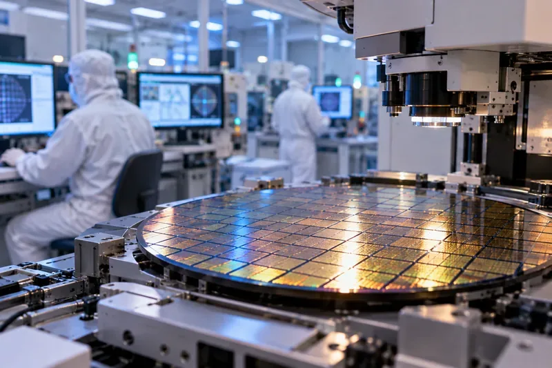
A silicon wafer sits on precision inspection equipment inside a semiconductor cleanroom, illustrating the manufacturing complexity behind leading-edge fabrication and advanced packaging.
The race now has two fronts: wafer fabrication and system-level packaging
Traditional semiconductor competition focused on front-end fabrication: transistor architecture, lithography, process control, defect density, and yield. Those factors remain fundamental. A weak process node cannot be rescued by clever packaging. But a strong process node alone is no longer enough for the largest AI and HPC designs.
Modern high-end chips increasingly use chiplets: smaller dies with different functions that are connected inside one package. A compute tile may use the newest logic node, while I/O, cache, analog, or interface functions can use other processes. High Bandwidth Memory, or HBM, is then placed extremely close to the compute dies so data can move with far more bandwidth and lower energy than it could through conventional board-level connections.
That architecture creates a new set of engineering bottlenecks. The package must provide very dense interconnects, control heat across multiple active dies, maintain power integrity, survive manufacturing stress, and be testable at useful yields. In other words, packaging has moved from being the final protective shell around a chip to being part of the chip's performance architecture.
A complex package can contain many expensive dies, so one bad element can be costly
TSMC is scaling both the transistor node and the package
TSMC remains the clearest example of how fabrication and packaging are becoming one roadmap. At its April 2026 North America Technology Symposium, the company said it was already producing 5.5-reticle-size CoWoS packages and planned a 14-reticle version for 2028. TSMC said that future configuration is intended to integrate roughly 10 large compute dies and 20 HBM stacks. Its roadmap also includes larger system-on-wafer approaches and tighter 3D stacking through SoIC. The details are in TSMC's 2026 technology symposium announcement.
This matters because the reticle size of a lithography system limits how large a single monolithic die can practically be exposed. Advanced packaging lets designers build systems larger than one reticle field by connecting multiple dies with high-bandwidth links. For AI accelerators, the result is a path to more compute and more HBM without forcing every function into one giant piece of silicon.
TSMC is also globalizing more of that stack. Its current Arizona project page says the planned U.S. investment has expanded to $265 billion and describes six semiconductor logic wafer fabs, two advanced packaging facilities, and an R&D center. It also states that the first advanced packaging fab entered initial construction stages in early 2026 and that the company announced further U.S. expansion intentions in July 2026. The latest project status is available on the official TSMC Arizona page.
For customers, the significance is not simply that more wafers can be made in the United States. If advanced logic is fabricated domestically but must still cross an ocean for the most sophisticated packaging, the supply chain remains geographically split. Bringing fabrication and packaging closer together can reduce that gap, although building a complete ecosystem also requires substrates, HBM, chemicals, tools, skilled labor, and test capacity.
Intel is betting on 18A plus packaging as a systems foundry strategy
Intel's strategy is different because it is trying to compete both as a processor company and as an external foundry. Intel says its 18A process is now in high-volume production in the United States and combines RibbonFET gate-all-around transistors with PowerVia backside power delivery. In June 2026, Intel also said 18A-P had entered risk production. The process details and current status are published on Intel Foundry's Intel 18A technology page.
But Intel is increasingly emphasizing the package around the node. EMIB uses small silicon bridges embedded in the package substrate to connect dies at high density without requiring a full-size silicon interposer. Foveros adds vertical stacking, and newer combinations aim to merge horizontal and vertical integration into larger heterogeneous systems. Intel's current advanced packaging portfolio describes EMIB, Foveros, Foveros Direct, and 3.5D combinations as part of that roadmap.
In June 2026, Intel also placed advanced packaging under dedicated foundry leadership, a structural change that reflects how strategically important back-end integration has become. The practical test is not the number of packaging names on a roadmap. It is whether outside customers can qualify designs, obtain predictable yields, ramp volume, and combine dies from multiple sources without excessive cost or schedule risk.
The United States is treating advanced packaging as industrial infrastructure
The U.S. government has also moved beyond a fabrication-only approach. In January 2025, the Department of Commerce finalized $1.4 billion in awards tied to the National Advanced Packaging Manufacturing Program, including funding for advanced substrates and materials as well as a packaging prototyping and piloting facility. The goal is explicitly to help move advanced packaging technologies from research into scalable domestic manufacturing. The award structure is described in the Department of Commerce announcement.
That policy shift is important because a country can have an advanced fab and still depend heavily on offshore assembly, substrates, packaging equipment, or memory. A resilient semiconductor supply chain is therefore not one factory. It is a network of wafer fabs, packaging plants, materials suppliers, tool makers, memory manufacturers, test facilities, and design ecosystems.
Samsung's advantage is the possibility of tighter logic-memory-package integration
Samsung approaches the race with a different set of assets: foundry manufacturing, advanced memory, and packaging technologies under one corporate umbrella. Its foundry business describes I-Cube solutions for 2.5D integration and X-Cube for 3D integration, with an emphasis on combining compute dies and HBM in heterogeneous systems. Samsung's official advanced packaging overview explains that strategy.
The potential advantage is coordination. AI processors depend heavily on HBM, and package design is closely linked to how many memory stacks can be placed around compute dies, how those dies are connected, and how the entire assembly is cooled. A company that can coordinate logic, memory, and packaging may be able to optimize the full system rather than treating each component as a separate procurement problem.
That does not automatically guarantee leadership. Customers still care about process maturity, design tools, ecosystem support, yield, capacity, and the freedom to combine components from different vendors. The global race is increasingly about offering the best complete manufacturing platform rather than the best isolated technology.
Europe is building shared pilot lines and packaging capacity
Europe's strategy is less about trying to duplicate every part of the Asian and U.S. ecosystems overnight and more about creating shared infrastructure that can move research into industrial use. In January 2026, the FAMES pilot line in Grenoble became the first of the five Chips Act pilot lines to become operational. In February, the EU opened the NanoIC pilot line at imec in Leuven with a total investment of €2.5 billion, including €700 million in EU funding. NanoIC focuses on beyond-2nm technologies and near-industrial experimentation. The European Commission's NanoIC announcement provides the funding and scope.
Packaging is explicitly part of the strategy. In March 2026, the European Commission granted Open EU Foundry status to Silicon Box's project in Novara, Italy, describing it as an advanced semiconductor packaging and testing facility that will integrate chiplets using panel-level packaging. See the Commission's Open EU Foundry decision.
The policy framework is still evolving. In June 2026, the Commission proposed Chips Act 2.0, aiming to reduce strategic dependencies and strengthen support for advanced chip production. Because that measure is a proposal rather than a completed legislative outcome, it should be read as a direction of travel, not as a finished funding or manufacturing guarantee. The proposal is available from the European Commission's Chips Act 2.0 page.
Japan is targeting the back end as well as advanced fabrication
Japan's semiconductor strategy is often discussed through leading-edge fabs and its strong equipment and materials ecosystem, but packaging is also receiving direct attention. On April 11, 2026, Japan's Ministry of Economy, Trade and Industry announced selected projects under its Post-5G program that included development of packaging technology for optical implementation in advanced semiconductor back-end processes. The original selection notice is on the METI program page.
Optical packaging matters because electrical links consume more power and become harder to scale as data rates increase. Co-packaged optics and other optical interconnect approaches aim to move data with lower energy per bit across short and medium distances. The technology is still evolving, but it is increasingly part of the packaging roadmap for AI infrastructure rather than a separate networking topic.
What technologies are most likely to decide the next phase
1. High-NA EUV and process control
Smaller features still require better lithography, metrology, masks, resist processes, and defect control. High-NA EUV can reduce patterning complexity on some layers, but the economic question is whether tool productivity, yield, and process integration justify the enormous capital cost.
2. Backside power delivery
As signal routing and power routing compete for space, moving power delivery to the backside of the wafer can reduce congestion and voltage loss. Intel is already using PowerVia on 18A, while other foundries are developing their own approaches. This is a fabrication innovation with direct consequences for package and system design.
3. Hybrid bonding and finer die-to-die pitch
Traditional microbumps consume space and add resistance. Copper-to-copper hybrid bonding can support much finer connections between stacked dies, increasing bandwidth density while reducing energy per transferred bit. The challenge is manufacturing precision, surface quality, alignment, and yield.
4. HBM integration and thermal engineering
For AI accelerators, memory bandwidth can be as important as raw compute throughput. More HBM stacks, larger compute complexes, and denser interconnects increase thermal density. Packaging leadership therefore depends on cooling, mechanical design, materials, and power delivery as much as on interconnect pitch.
5. Test and known-good-die strategy
A package containing multiple expensive dies magnifies yield risk. Manufacturers need to identify bad dies before assembly, test interconnects after bonding, and diagnose failures in structures that may be difficult to probe directly. Better test methodology can have a major effect on the economics of chiplet systems.
What this race means for AI and cloud buyers
For a data-center operator, the semiconductor race shows up as more than benchmark scores. Packaging capacity can affect accelerator availability. HBM integration affects memory bandwidth and usable model size. Thermal design affects rack density and cooling requirements. Process efficiency affects electricity consumption. Geographic diversification can influence lead times and supply continuity.
That means buyers should evaluate accelerators as systems. A nominally faster compute die is not necessarily the better platform if the memory subsystem is constrained, the package runs hotter, or supply is limited by a specialized packaging step. Likewise, a chip manufactured on a slightly older node can remain highly competitive if its package architecture, memory bandwidth, software stack, and power efficiency are stronger.
What to watch through 2027 and 2028
Actual volume ramps, not just roadmap dates. Watch which advanced nodes and package technologies ship in sustained customer volume.
Packaging yield and capacity. CoWoS, EMIB, Foveros, I-Cube, X-Cube, hybrid bonding, and panel-level packaging matter only if they can be produced economically at scale.
HBM supply and package co-design. The memory and package roadmaps are increasingly inseparable for AI hardware.
Co-packaged optics. The technology could become important as electrical I/O power becomes a larger part of system energy use.
Regional completeness. New fabs are strategically valuable, but the stronger question is whether a region also has substrates, packaging, test, memory, tools, chemicals, and skilled workers.
Open chiplet ecosystems. The more easily designers can mix dies from different vendors and process nodes, the more flexible advanced packaging becomes as an alternative to monolithic chips.
The bottom line
The global semiconductor race in 2026 is not a single contest with a single winner. TSMC is combining aggressive leading-edge fabrication with rapidly expanding 3DFabric and CoWoS capabilities. Intel is trying to pair 18A-class manufacturing with a differentiated packaging stack and a U.S.-centered foundry model. Samsung can combine foundry, memory, and advanced packaging. Europe is building shared pilot infrastructure and new packaging capacity, while Japan is investing in back-end and optical integration technologies alongside its broader semiconductor base.
The most important shift is conceptual: the package is now part of the processor. Future performance gains will come not only from shrinking transistors, but from placing the right compute, memory, I/O, and optical components together with enough bandwidth, power efficiency, cooling, yield, and manufacturing capacity to make the design economical. The companies and regions that master both fabrication and heterogeneous integration will have the strongest position in the next generation of AI and high-performance computing.