Home
» New Trends
»
How Silicon Innovation Is Driving the Next Industrial Revolution
How Silicon Innovation Is Driving the Next Industrial Revolution
Calling today’s semiconductor boom the “next industrial revolution” can sound like marketing shorthand. Yet the underlying shift is real: factories, vehicles, data centers, power systems, robots, medical equipment, and communications infrastructure are becoming more dependent on specialized computing and power electronics. The important point is not that silicon alone is transforming industry. It is that advances in transistor design, lithography, packaging, sensing, memory, and power semiconductors are making more computation and control practical inside physical systems.
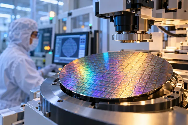
A patterned silicon wafer sits beneath precision inspection equipment in a semiconductor cleanroom, illustrating the manufacturing foundation behind increasingly capable industrial computing and control systems.
This distinction matters because several common assumptions about semiconductor progress are too simple. Some claims are well supported by current manufacturing milestones. Others depend heavily on application economics, software, thermal design, supply chains, and integration quality. And some of the biggest promises—such as fully autonomous factories or dramatic economy-wide productivity gains—remain uncertain.
What “silicon innovation” actually means in 2026
Silicon innovation is no longer synonymous with shrinking one monolithic processor. Modern progress comes from several layers working together. Leading-edge logic still matters, but so do new transistor structures, backside power delivery, advanced lithography, chiplets, high-bandwidth memory, 2.5D and 3D packaging, silicon photonics, analog chips, sensors, and power devices.
A useful example is Intel 18A. Intel says the process combines RibbonFET gate-all-around transistors with PowerVia backside power delivery, and it entered production in 2025. In June 2026, Intel reported that the performance-enhanced 18A-P variant had entered risk production. Those are concrete manufacturing milestones, not merely roadmap concepts. See Intel’s Intel 18A process overview and its June 2026 process update.
Action: When evaluating a new chip platform, look beyond the process-node label. Ask for workload-level data on performance per watt, memory bandwidth, thermal behavior, package size, reliability, and production maturity.
Misconception 1: Smaller transistors are the whole story
What is verified
Transistor scaling continues to matter, but the industry is also changing how power and interconnects are arranged. ASML announced on July 15, 2026 that Intel Foundry was using High NA EUV on selected Intel 18A layers for a subset of high-volume products, describing it as an important readiness milestone for more precise patterning. High numerical aperture extreme ultraviolet lithography is intended to extend patterning capability for future advanced nodes. The underlying milestone is documented in ASML’s High NA EUV production-readiness announcement.
What depends on context
A more advanced lithography tool or denser process does not automatically make every industrial product better. Many factory controllers, motor drives, sensors, and safety systems prioritize long service life, deterministic behavior, temperature tolerance, qualification history, or cost over maximum transistor density. Mature process nodes can remain the better engineering choice for years.
What is still unknown
The long-term cost curve for each new manufacturing generation is not predetermined. Yield learning, tool productivity, design complexity, energy use, and packaging costs all influence whether a nominally more advanced node produces a better total system.
Action: Match semiconductor technology to the product’s actual bottleneck. If the constraint is compute density, advanced logic may be decisive. If the constraint is high voltage, thermal stress, analog precision, or product lifetime, another technology may create more value.
Misconception 2: Packaging is just the protective shell around a chip
What is verified
Advanced packaging has become part of the computing architecture itself. TSMC’s CoWoS platform integrates logic and high-bandwidth memory using large interposers and other high-density interconnect methods. TSMC says CoWoS has been in volume production since 2012 and that demand increased significantly with generative AI. Its current platform description is available on the company’s CoWoS technology page.
The U.S. National Institute of Standards and Technology also treats advanced packaging as a strategic manufacturing capability. NIST describes it as assembling diverse chips closely in two or three dimensions so that a system can gain performance and power benefits beyond conventional board-level integration. See the National Advanced Packaging Manufacturing Program.
What depends on context
Chiplets and 3D integration can improve modularity and bandwidth, but they introduce new engineering problems. Die-to-die links consume power. Dense packages create thermal hotspots. Testing becomes harder when multiple dies interact. Yields, known-good-die strategies, substrates, and cooling design can determine whether the architecture is economical.
What is still unknown
There is no universal winning chiplet architecture for industrial systems. Interoperability standards, package ecosystems, and long-term repair strategies are still evolving, especially outside hyperscale computing.
Action: Treat package architecture as an early design decision, not a back-end detail. For compute-intensive products, evaluate die partitioning, memory placement, interconnect bandwidth, thermal limits, test strategy, and supply risk together.
Misconception 3: AI is the only reason industrial demand for chips is accelerating
What is verified
AI is a major demand driver, but industrial semiconductor growth is broader. NIST’s July 2026 Roadmap on Artificial Intelligence and Machine Learning for Smart Manufacturing identifies applications including advanced sensing, robotics, digital twins, industrial analytics, autonomous systems, supply-chain optimization, and sustainable manufacturing. These capabilities rely not only on AI accelerators but also on sensors, microcontrollers, networking, memory, analog electronics, and power management.
Industrial electrification is another major thread. The U.S. Department of Energy has highlighted silicon carbide power electronics as an enabling technology for more efficient next-generation electric machines and motor drives. Its overview, Get Your Motor Running: The Next Generation of Electric Machines, describes work combining advanced motors with SiC-based power conversion.
What depends on context
Running AI at the edge can reduce latency and cloud dependence, but it is not automatically cheaper or more reliable. Industrial deployments must account for sensor quality, model drift, cyber risk, real-time constraints, maintenance practices, and the cost of validating decisions in safety-critical environments.
What is still unknown
There is not yet enough evidence to assume that adding AI hardware to a machine or production line will produce a predictable productivity gain. Results vary by process stability, data quality, operator workflow, integration quality, and whether the automation addresses a meaningful bottleneck.
Action: Start with a measurable operational problem—such as scrap rate, unplanned downtime, inspection delay, energy consumption, or cycle-time variation—then choose the compute architecture that can improve that metric. Do not begin with “we need AI chips” as the requirement.
Misconception 4: Silicon carbide is simply replacing silicon
What is verified
Silicon carbide, or SiC, is a compound semiconductor that can outperform conventional silicon devices in many high-voltage and high-frequency power-conversion applications. Infineon positions SiC MOSFETs for industrial drives, renewable-energy systems, uninterruptible power supplies, electric-vehicle charging, and other power-intensive uses. The company’s industrial motor-drive overview explains why SiC can be attractive where switching performance and power density matter.
What depends on context
SiC is not universally superior. Conventional silicon MOSFETs, IGBTs, and integrated power devices remain highly competitive across many voltage, frequency, cost, and reliability ranges. The best choice depends on switching frequency, bus voltage, thermal design, efficiency target, cooling cost, expected duty cycle, and component availability.
What is still unknown
Future price gaps among silicon, SiC, and gallium nitride devices will depend on manufacturing scale, wafer supply, yields, packaging, and demand. No responsible technology plan should assume that today’s price relationship will remain fixed.
Action: Compare technologies using system-level total cost rather than device price alone. Include cooling hardware, passive components, enclosure size, energy losses, maintenance, qualification effort, and expected service life.
Misconception 5: More semiconductor capacity automatically creates a resilient supply chain
What is verified
Governments and industry are investing in domestic semiconductor R&D, packaging, and manufacturing capacity. In the United States, NIST’s CHIPS programs explicitly target advanced packaging, metrology, manufacturing research, and faster transfer from prototype to commercial scale. In July 2026, the Department of Commerce also announced letters of intent totaling up to $874 million for R&D projects spanning advanced memory, packaging, photonics, substrates, and related compute technologies. The announcement is documented by NIST in its July 29, 2026 CHIPS R&D release.
What depends on context
Resilience depends on more than wafer-fab capacity. A product can still be exposed through substrates, advanced packaging, specialty chemicals, photomasks, electronic-design-automation software, memory, test equipment, or a single qualified component. A geographically diverse fab footprint does not eliminate single points of failure elsewhere.
What is still unknown
The semiconductor industry is building capacity against rapidly changing demand, especially from AI infrastructure. It remains difficult to know which segments will be constrained or oversupplied several years from now. Long construction cycles make perfect matching impossible.
Action: Build a supply-chain map at the component and process level. Identify single-source parts, sole-source packages, long qualification cycles, and dependencies on one region or manufacturing technology. Then prioritize second-source qualification where downtime would be most expensive.
Where silicon innovation is most likely to reshape industry
Area
What is already credible
What still depends on execution
Useful next move
Smart factories
More capable sensing, edge compute, machine vision, robotics, and industrial AI
Data quality, deterministic control, cybersecurity, and integration with legacy equipment
Pilot on one constrained production cell and measure a business KPI
Industrial power
Higher-efficiency switching using silicon, SiC, and other power-semiconductor technologies
Economics vary with voltage, load profile, cooling, and operating hours
Run a lifecycle energy-and-cooling cost model before redesigning hardware
AI infrastructure
Advanced logic, HBM, networking, and packaging are enabling denser computing systems
Power delivery, cooling, software efficiency, and infrastructure cost can become limiting factors
Optimize the entire rack or system rather than comparing accelerator chips alone
Robotics and autonomous machines
More compute can move closer to cameras, sensors, and actuators
Reliability, safety validation, perception quality, and operating environment remain decisive
Separate tasks that truly require local inference from tasks that can remain centralized
Transportation and energy
Power electronics and embedded control improve electrified systems
Benefits vary by architecture, duty cycle, charging or grid design, and thermal constraints
Evaluate efficiency at the full system level, not only at the semiconductor level
The deeper shift is from chips to systems
The strongest evidence for a new industrial phase is not one spectacular transistor breakthrough. It is the convergence of several technologies that let engineers place more intelligence, sensing, connectivity, and power control inside physical equipment.
That convergence is visible in advanced-node manufacturing, in High NA lithography milestones, in tightly integrated multi-die packages, in edge AI roadmaps, and in the expansion of SiC power electronics. It also explains why semiconductor strategy is becoming a board-level industrial issue rather than a purchasing detail.
But the phrase “next industrial revolution” should not be treated as a measurable technical milestone. It is a useful description of a direction, not proof that every industry will transform at the same pace. Adoption will be uneven. Some sectors can refresh hardware every few years; others must qualify systems for decades. Some processes generate clean digital data; others still depend on noisy sensors, manual workarounds, and legacy controls.
Action: Build technology roadmaps around system constraints rather than trend labels. For each product or production line, identify the limiting resource—compute, memory bandwidth, power, latency, thermal headroom, sensing quality, reliability, or supply risk—and then decide whether new silicon technology meaningfully changes that constraint.
What industrial leaders should watch next
Over the next several years, the most important signals will be less about headline transistor counts and more about manufacturability. Watch whether High NA EUV broadens beyond early production use, whether advanced packaging capacity keeps pace with high-bandwidth-memory demand, whether chiplet standards become easier to deploy across vendors, and whether power-semiconductor cost and qualification improve enough to expand into more industrial drives and grid equipment.
Also watch the software layer. Faster silicon creates value only when compilers, operating systems, industrial protocols, model runtimes, safety tooling, and maintenance processes can use it reliably. In factories especially, a modest processor with predictable real-time behavior can be more valuable than a faster accelerator that is difficult to validate or maintain.
The industrial significance of silicon innovation is therefore not that every machine is becoming a computer. It is that the boundary between computation and physical infrastructure is disappearing. The companies that benefit most will be those that evaluate semiconductor advances as part of complete systems—technical, economic, operational, and supply-chain systems—rather than as isolated chips.